Long time no post! Now that’s out of the way… As ever, I’m always on the search for cheap electronics and this board is nearly mind blowing given both the price and form factor you can get it in. Enter the Gnarly Grey UPDuino v2.0 based on a Lattice iCE40UP5K FPGA featuring:
- 120Kbits of BRAM
- 1024Kbits of Single Port RAM
- Integrated PLL
- Integrated DSP units (MAC!)
- I2C and SPI IP
- Internal HF and LF oscillators
- LED driver
- PWM IP blocks
- 48pin QFN
A pretty feature packed little guy for only $15.99. I’ve been looking for an FPGA of this size and form factor for a very long time and finding one at this price just so happens to be a bonus.
The cheap price however comes with a few niggles, namely getting it up and running in the first place with the limited documentation. Gnarly Grey do a great job of explaining programming a starting program but don’t say much about further development. With that in mind, I’m going to run through the methodology of getting an LED flashing using VHDL. There seem to be a fair few Verilog methods but not many people seem to have touched upon VHDL with these FPGAs.
Pre-requisites
I’m assuming iCECube2 and Lattice Diamond Programmer are already installed. Gnarly Gray has a programming document on their Github which states the required software for installation.
Making a project
First things first, a project needs to be made. Open up iCECube 2 and double click “New Project”.
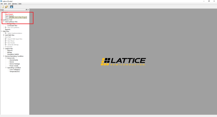
Create a new project
In the new project window, select iCE40UP, ensure 5K is selected along with the SG48 package. Finally, select the bank voltage. The default jumper position for this is 3.3V.
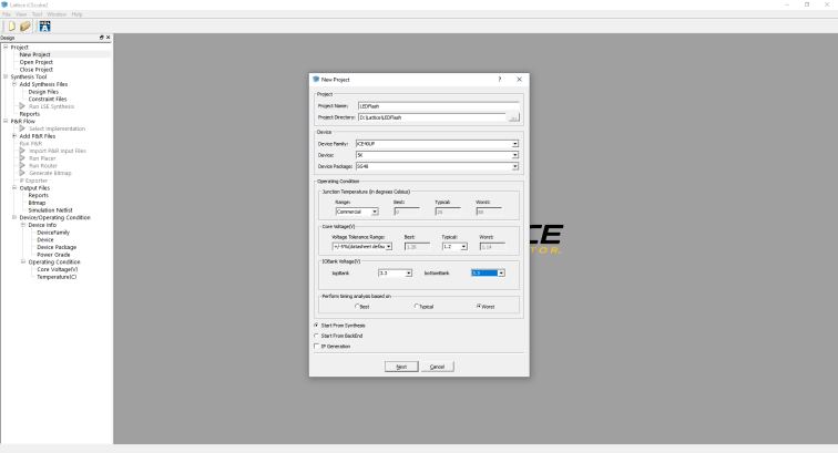
Set up project settings
Clicking next will show prompt windows, one of these being add files. As no files have been written yet, no files need to be added. After following the prompt windows, you should arrive at the normal project screen with the output window open.
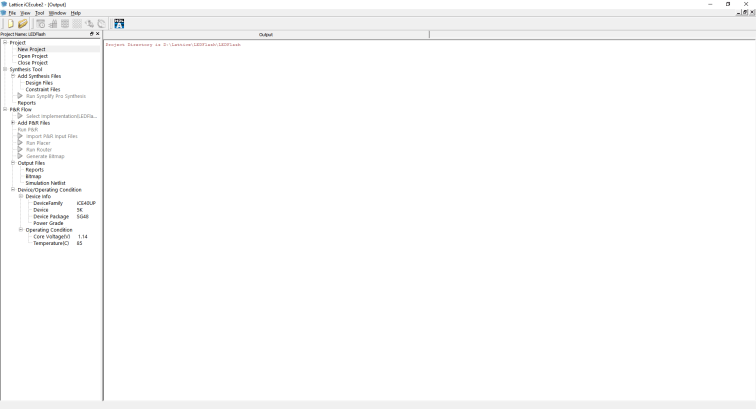
Output screen after creating a project
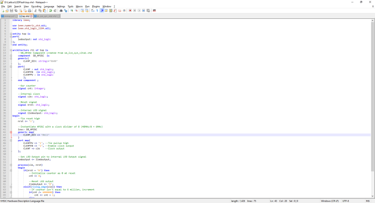
Now the project has been created, coding can begin! For this program, I’m going to use HFOSC (internal oscillator) operating at 6MHz and an LED connected to pin 2. The program is going to have a counter that counts to 6 million then toggles the LED. Obviously this is quite a simple program but figuring out how to correctly instantiate HFOSC is the hardest part. The code for this is:
Code
library ieee;

use ieee.numeric_std.all;
use ieee.std_logic_1164.all;

entity top is
port(
	ledoutput: out std_logic
);
end entity;

architecture rtl of top is
	--SB_HFOSC Component created from sb_ice_syn_vital.vhd
	component  SB_HFOSC  is
	generic(
		CLKHF_DIV: string:="0b00"
	);
	port(
		CLKHF : out std_logic;
		CLKHFEN  :in std_logic;
		CLKHFPU : in std_logic
		);
	end component ;

	--Our counter
	signal cnt: integer;

	--Internal clock
	signal clk: std_logic;

	--Reset signal
	signal nrst: std_logic;

	--Internal LED signal
	signal iledoutput: std_logic;
begin
	--Tie reset high
	nrst <= '1'; 	 	--Instantiate HFOSC with a clock divider of 8 (48MHz/8 = 6MHz) 	iosc: SB_HFOSC 	generic map( 		CLKHF_DIV => "0b11"
	)
	port map(
		CLKHFPU => '1',	--Tie pullup high
		CLKHFEN => '1',	--Enable clock output
		CLKHF => clk	--Clock output
	);

	--Set LED Output pin to internal LED Output signal
	ledoutput <= iledoutput;

	process(clk, nrst)
	begin
		if(nrst = '0') then
			--Initialize counter as 0 at reset
			cnt <= 0;

			--Reset LED output
			iledoutput <= '0';
		elsif(rising_edge(clk)) then
			--If counter isn't equal to 6 million, increment
			if(cnt /= 6000000) then
				cnt <= cnt + 1;
			else
				--Reset counter
				cnt <= 0;

				--Toggle LED
				iledoutput <= not iledoutput;
			end if;
		end if;
	end process;
end rtl;
The best IDE… Notepad++ 😉
The above code should be saved as the top entity.
Once the code has been written, a pinmap describing what ports map to each pin needs to be created. This can also be done in Notepad++ and needs to be saved as a .pcf file. As we only have one output pin, this file will contain one line of text.
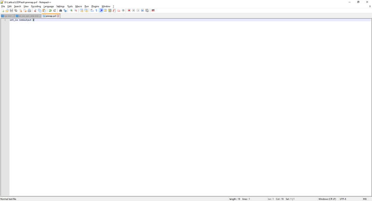
Creating the pinmap file
Now these files have been created, we can start with synthesis and routing!
Synthesis
In iCECube2, import the top file by navigating to Add Synthesis Files, right clicking and selecting Add Files. Navigate to the project folder and select top.vhd.
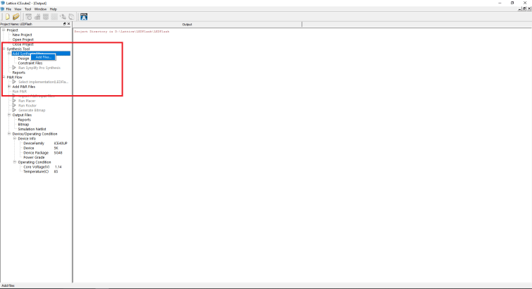
Add files to the project
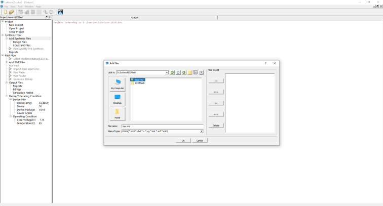
Select top file
Once the file has been selected, press >> to add it to the current project and press Ok.
We can now start the synthesis! Double click Run Synplify Pro Synthesis. If all goes well, the synthesis should be successful and no errors should be present in the output window.
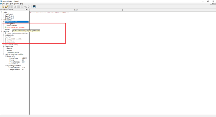 Initialize the synthesis
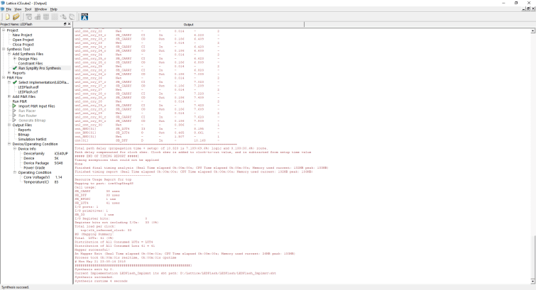
Synthesis outputs
P&R
Now the synthesis has been completed and was successful, the pinmap file can be added and placing and routing can begin. To add the pinmap file, navigate to Add P&R Files, right click and select Add Files. Once again, navigate to the project folder and select the pinmap file. Add this file to the project using the >> button. Finally start the P&R by double clicking Run P&R.
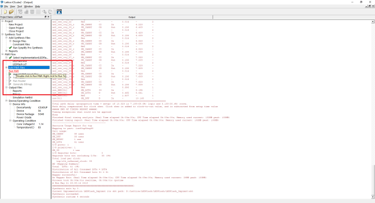
Start place and route
If all has gone well, P&R should be successful and you should have green ticks next to all tasks in the project window.
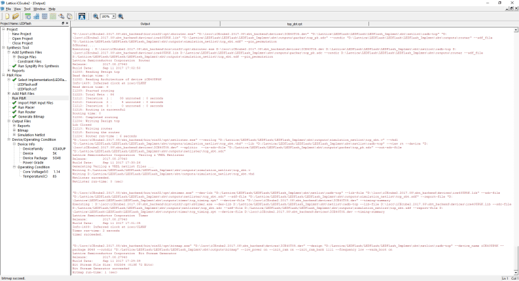
Success! Synthesis and P&R were fine.
The generated bitmap can now be uploaded to the FPGA using the Diamond Programmer.
Programming
Gnarly Gray has good instructions on programming but I will elaborate here with images.
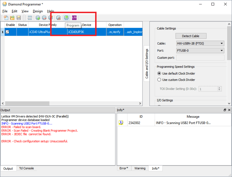
Firstly, open Diamond Programmer. A getting started window should pop up with the programming device selected. Clicking Detect Cable should select the correct programmer for you.
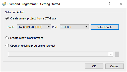
Getting started window
This window can be closed by pressing Ok. This will then bring up the main programming window. An initial scan will happen and likely find nothing as no parameters have been set. Once the scan has finished, you should be left with an open screen.
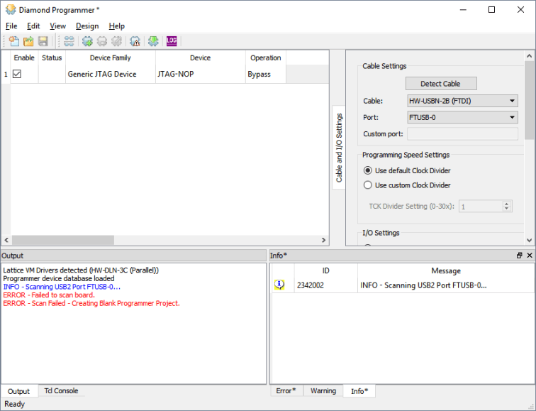
Programming window with failed initialization
In this window, you will want to select iCE40 UltraPlus on the Device Family drop down list.
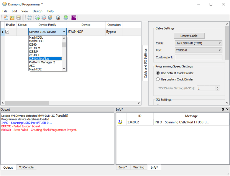
Select correct device
In this case, you will also want to select iCE40UP5K as the device too. Next, you will want to initialise the programming parameters. This can be done by double clicking the box underneath Operation.
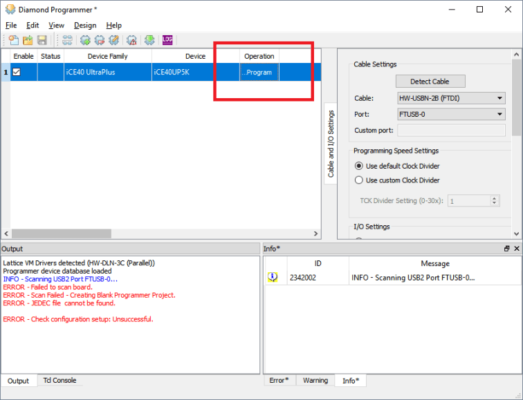
Open programming parameter window
In this window, you will want to set Access Mode to SPI Flash Programming. This should expand the window. Next, you will want to select the programming file by pressing the three ... next to the Programming File text box. Here you will want to navigate to the synthesized output folder which should be found at: …\LEDFlash\LEDFlash\LEDFlash_Implmnt\sbt\outputs\bitmap where … is the project root folder. Select top_bitmap.hex and press Ok.
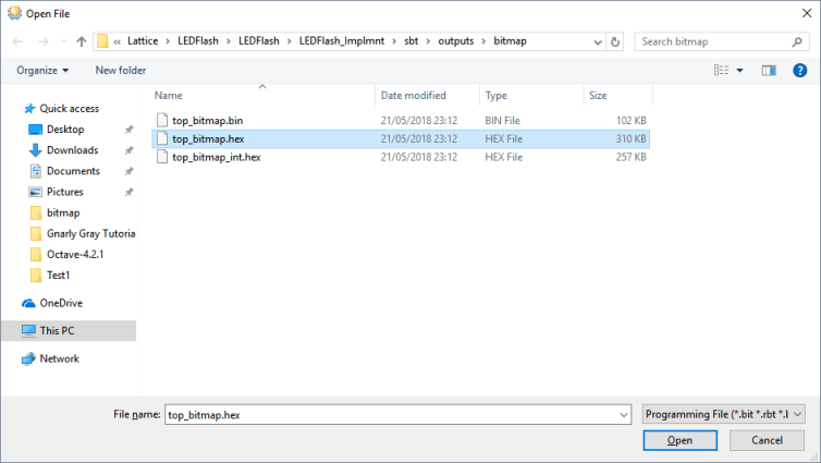
Select programming bitmap file
Next, you will want to select the correct SPI Flash chip. This would be the Numonyx SPI-N25Q032 8-pin VDFPN8 version.
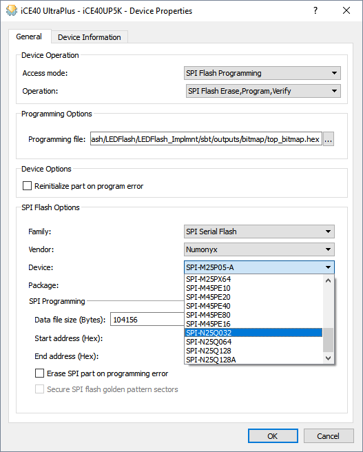
Select target SPI Flash
This window can now be closed by pressing Ok. Finally, the chip can be programmed by pressing the program button.
Program the flash!
Upon programming, you should see the LED flashing indicating the program is a success!
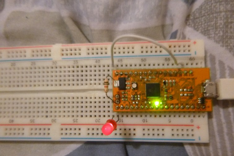
Success! A flashing red LED.
Voila! Your first Gnarly Gray project from scratch.

Thanks for doing this. I’m a newbie and I can’t make a lick of sense out of Verilog. (What were they thinking?) The Lattice documentation is so awful, that I didn’t have a chance sorting out SB_HFOSC on my own.
Your code also works fine on the Lattice iCE40UP breakout board. (But the screen prints in your article are way too small. I couldn’t read any of them even zoomed in.)
I completely agree about the documentation, its absolutely abysmal. I had to figure it out reading through the source. They do mention HFOSC in one of the hardware manuals but don’t actually give a VHDL implementation! I’ll have a look to see if I can improve the quality of the shots now, thanks!
(Sorry, some of the screen shots are quite readable.) Next, I ran into another road bump with sb_rgba_drv. Then I found this:
https://stackoverflow.com/questions/50276929/using-the-sb-rgba-drv-primitive-in-vhdl
There isn’t a lot of documentation on fpgas to begin with, atleast easy to read. Heck, as of 2019, I am trying to figure out if I need to use Cube2 or one of their other software for more features? Sigh.
Any idea on how to get Lattice to respond to a request to D/L IceCube2? They seem to have put it behind a paywall/request wall. I have created an account well over 2 months ago and emailed their support but no one has reached back out…