As some of you might know, one of my main most favourite hobbies ever is playing bass! When bass playing and electronics mix, the end result is generally either the Phobass or bass effects pedals! I had previously made many pedals in the past and two were consistent additions to my pedal board but stupidly, I left it on a train once (VERY stupidly!). So I’ve been deciding upon my new arsenal of pedals and the first I’ve designed is a simple splitter pedal, 1 bass goes in, 4 volume controllable bass’ come out!
I’d decided to use a new PCB manufacturing company for this board, as its not particularly critical! I ended up finding one source on ebay where UK manufactured PCB’s were £2.50/PCB Unit (defined in the listing: http://goo.gl/U4haC1 LINK WILL EXPIRE! Auction name: PCB Printed Circuit Board Prototype Production/Milling/Manufacture/Manufacturing). The quality of the PCB was brilliant but it didn’t occur to me that I’d need to link up the via’s as the service only provides the PCB milling.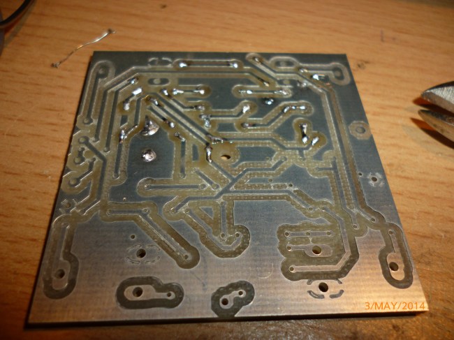
Milled PCB with half of the via’s “filled”
Linking the via’s was actually relatively easy as it just consisted of putting stripped kynar wire through the hole, soldering it on both sides and snipping it off!
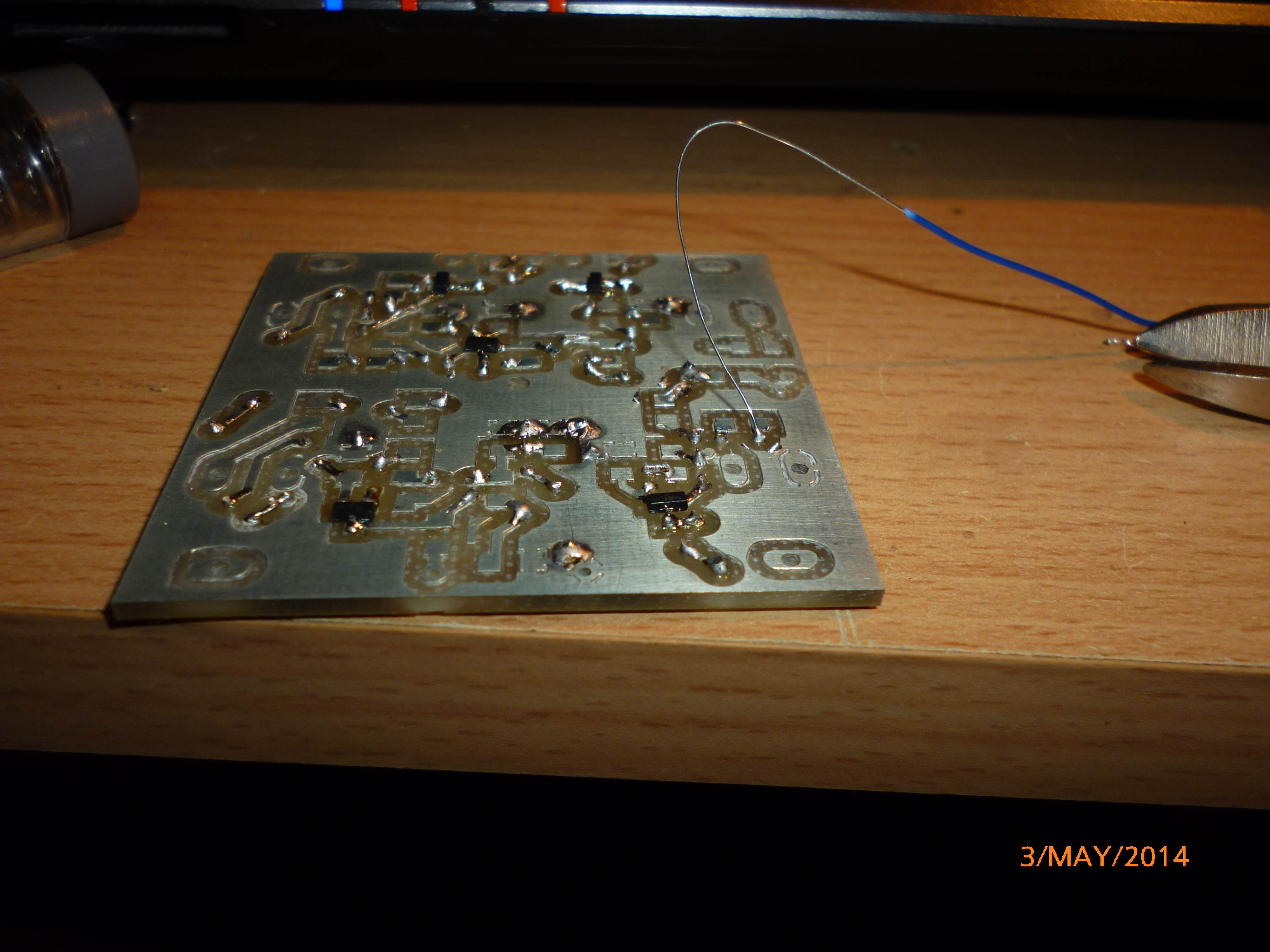
Creating the through part of the vias
Another thing I didn’t realise is that it wouldn’t have solder mask or silk screen! The silk screen wasn’t a massive problem as I normally make PCB’s along side having eagle open displaying components but having no soldering mask made construction a bit more complex to normal as components could move, solder bridges could be easily made etc. Once I’ve completely finished the board, I’ll probably paint the traces with nail varnish as this normally gives a good insulated layer.
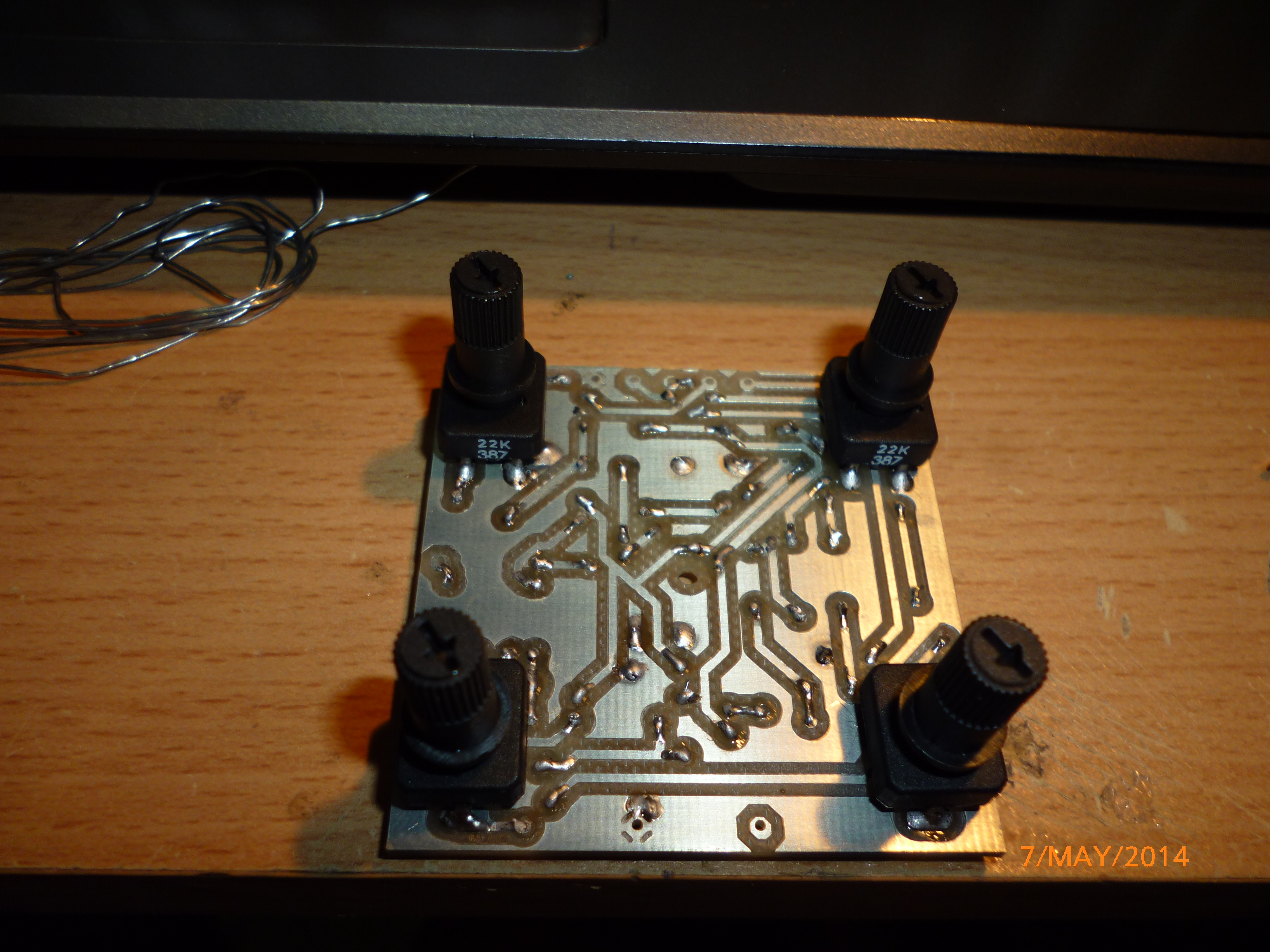
Soldering on the volume pots
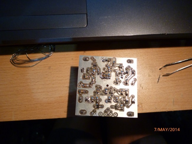
Finished solder side with components! Its less scruffy than it looks IRL, honest!
Keep tuned for a potential video update!
