The magic 3! FPGAs being the coolest components out there, with VGA being the standard for all graphics and finally; SDRAM, the base of all synchronous memories.
These past few days, I’ve been designing an FPGA based SDRAM controller as I’ve got an SDRAM chip on my FPGA development board which I haven’t yet interfaced to. Instead of going down the route of finesse with good interleaved bank and row management, I instead decided to go down the brute force route with wide memory buses and large potential latencies. My SDRAM chip is a Winbond W9825G6JH-6 with 32MB of accessible memory. I’ve never written an SDRAM controller before so it was definitely an interesting task to learn. The chip supports bursts up to 8 words of length meaning 128bits (16bits*8) of data in a single read of write transaction can be transferred.
Currently, rows are activated, accessed (read/written) and precharged straight after the operation. Refreshes are commanded every 7us as worst case read/write time is ~0.2us (a refresh should be roughly every 7.2us – 64ms/8,192). Using this brute force 128bit memory access method with a memory clock of 100MHz, I can achieve read speeds of 65.8MB/s and write speeds of 75.5MB/s. I ran a full memory test over night at this speed and found no memory errors.
Memory test
The memory test is relatively simple. A simple state machine writes a variable (data counter) to the SDRAM. Once written, this value is incremented and written to the next location. This is done until the entire memory array has been written. Once the entire memory array has been written, the data counter is reset to zero. The data counter is compared to every word read back and incremented after every read. Any differences force the state machine into an error state. I left this on over night and throughout the day (around 16 hours) with no single errors!
VGA Interface
I’ve written multiple VGA interfaces previously, some with memory, some without. Driving a VGA monitor is actually a really easy task and generally only needs two timers and some logical comparators. In this instance, I’ve written a pretty generic module that can work for any VGA resolutions if the correct clock frequency, porch and sync lengths and pixels etc. are supplied. My board features an 16bit R2R DAC connected between the VGA port and the FPGA allowing RGB565 video to be displayed.
As one pixel is 16bits and my memory interface is 128bits wide, this allows for 8 pixels to be transferred per memory transaction. This means the actual memory access clock can run at 1/8th of the pixel clock.
Implementation
 RTL diagram of the total system
Rsthandler
This is a simple module that debounces the reset switch. It consists of a long counter that is reset every time a button is pressed. Once the counter reaches all ones, the output goes high, otherwise the output is low, resetting all modules.
Memhandler
This module is used to cross the clock domain between the pixel clock and memory clock and grabs the pixels for the VGA controller
Seg7
This is a simple module which displays a 4 digit hex number on the on board 7 segment display.
VGA
This is the actual VGA controller and requests pixels from the memory handler, finally spitting them out into the DAC.
SDRAMCtrl
This module generates the signals required to interface an SDRAM module. The module interfaces the memhandler through a single clock enable interface. With the enable signal high, the value present on the “wr” input depicts the action. A ‘1’ on wr will initiate a write operation whereas a ‘0’ on wr will initiate a read operation. On the falling edge of the bsy signal, data on the “do” port will be what was read from the memory.
Performance

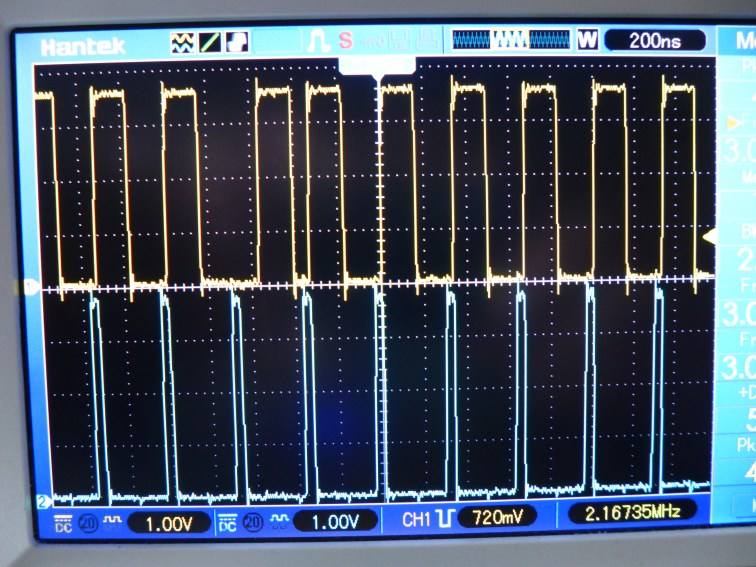
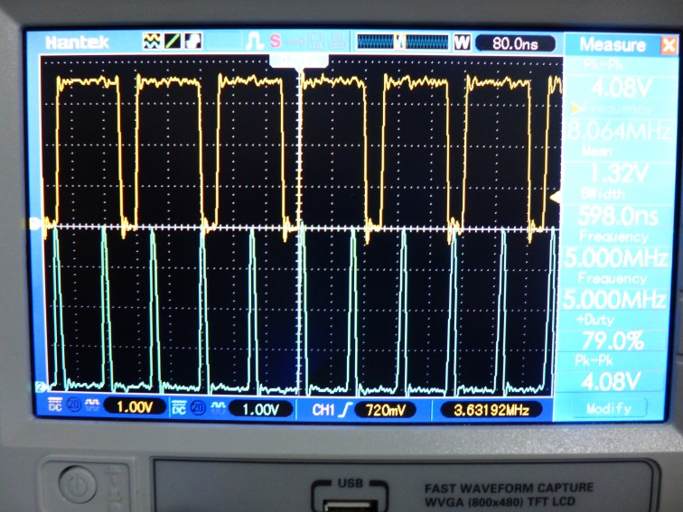
Monitoring the memory access vs pixel request
As a method of analysing how occupied the memory controller is and how bad pixel latency is, I’ve brought out the pixel request signal, along with the memory handler busy signal. The memory request is the blue trace and the busy signal is the yellow trace. As can be seen, the memory access is around 50% during a line and is obviously zero during blanking. Upon reset, the memhandler initializes the SDRAM with an incremented value producing a colour gradient image on the screen.
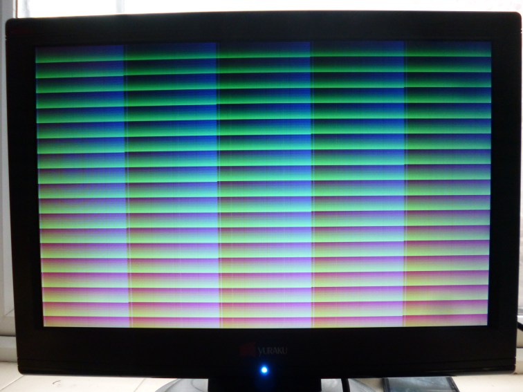
The ol’ colour gradient!
There are a couple of artifacts that can be seen above and a bit of jitter when a refresh occurs at the wrong moment but all in all, 640×480 seems to work!
Visible memory access jitter due to a refresh cycle. As can be seen, the pixel is accessed just much later than it should’ve been.
Higher resolutions
As a test of how much further I could push my memory controller, I decided to test higher resolutions.
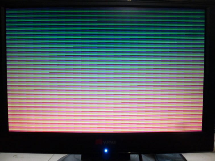
 Testing the memory access at 800×600
As can be seen, 800×600 is pushing it a touch with memory access at ~70% with minimal time free after the pixel has been provided.
 Testing at higher resolutions
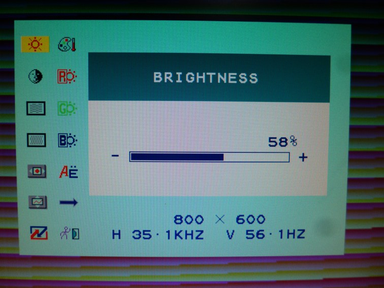
800×600, honest!
1024×768
Testing at 1024×768
At this resolution however, it can be seen that memory access is too slow compared to pixel requests, generally missing pixels. This produces many artifacts.
 Visual artifacts due to incapable memory access.
I’m yet to code the memory arbitrator to allow access during blanking. Sadly, I’ve nearly completely ran out of pins on this FPGA so all I’ll probably be able to do is either make a UART interface or a simple SPI interface.
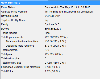
Synthesis
Surprisingly, the synthesis is quite small with a total consumption of:
I wouldn’t recommend the code but it can be found on my Github!
